: Not shown: crystals, decoupling caps, VCO for the FPGA? 2.0 V supply for the CPU?
Historical interest only: unchanged since October 1999
Not that I think SNS should build something like this, rather we would like to convince someone else to build it, and sell it to us. In cases like this, where a project invests time and infrastructure in using a commercial product, I think that product's design should go into escrow (held by a neutral third party). The design would be released if a problem arose delivering the product at an agreed upon schedule and price.
Patterned after the uCsimm, which looks nice but is underpowered for this purpose. The TINYCORE Module is a similar concept, but I don't think the 80960 is supported by gcc, and the FPGA is part of the computer design, not available for the application. A User-mode FPGA for the IEEE-1386.1 mezzanine slot is sold by Technobox. Some interesting single board computers, including FPGA? are sold by Applied Data Systems. The Bright Star Engineering ipEngine looks really close in concept to this discussion, although they chose a CPU (the Motorola MPC823) that has a rather strange feature set.
We want a high density, widely available connector, with 50-100 pins. Suppose we can use a 72-pin SIMM interface. Dedicate approximately 12 of those pins to power and ground (this is a major failing of the uCsimm in my view -- it's useless for high frequency work because there aren't enough ground pins).
The following special purpose pins are useful when directly connected from the CPU (or Ethernet chip) to the edge of the SIMM:
That leaves approximately 47 pins for "User I/O", in fact routed directly to the FPGA. All other special-purpose and general-purpose I/O pins on the SA-1100 would go to the FPGA. That chip could be programmed to act as a transparent buffer, if the unaltered functionality were wanted off-board.
The FPGA programming needs to be controlled from the computer, and the computer has to come alive and onto the net without help from the FPGA. To accomplish this, approximately four general purpose I/O pins from the computer have to be connected to the serial programming port of the FPGA.
The SA-1100 needs 32.768 kHz and 3.686 MHz crystals. It can directly support (glueless) the DRAM and Flash. The trick for the Ethernet and FPGA is to consider them PCMCIA devices. Since they are on board, no buffers are needed. The FPGA comes up high impedance (weak pull-up), which is OK to hang on the bus, it's not that different from a disabled PCMCIA device. Programming the chip is equivalent to plugging in a PCMCIA card, although a buggy FPGA program can crash the computer by driving the bus at the wrong time.
Condensed SA-1100 options:
The voltage listed is for the core, all varieties use 3.3 V for I/O. All the other chips in the computer use only 3.3 V supplies. The final "x" in the part code is "A" for the 208 pin TQFP, and "B" for the 256 ball mBGA.
Other CPU chips worth considering:
Flash chips:
That Ethernet chip needs a 20 MHz crystal. The transformers needed to connect it to 10BaseT (RJ-45) would go off-board. No EEPROM is needed in this case, configuration data can be held in the system Flash. Even better would be to take information from off-board, like the Dallas Semiconductor DS2401 serial number chip. This way the computers on the net would all be interchangable without any setup (MAC derived from the serial number, IP derived from MAC by rarp, EPICS and FPGA configuration based on IP). Better allocate a couple off-board pins for direct processor digital I/O (without the FPGA) to allow this.
Micron has a nice page of . . DRAM info:
both shipping now. They also have 32-bit wide RAM, but that is considered "specialty", and therefore probably needlessly expensive. That 50 pin TSOP has a 21x12 mm footprint, 0.80 mm pitch leads.
Package sizes in mm, prices in US$ where known:
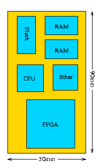
To-scale (but not necessarily realistic) representation of the size of the
computer:
:
Not shown: crystals, decoupling caps, VCO for the FPGA?
2.0 V supply for the CPU?
SIMM/DIMM boards, and their approximate clear area:
Note that at least some SIMM/DIMM sockets are only rated at 25 cycle durability.
Other possibly relevant connectors:
The setup just described puts the FPGA within the single board computer, and in fact right on the processor data bus. This clearly has the shortest latency and highest throughput of any means of connection. The wide, parallel interconnect between the CPU and FPGA is contained on one PC board (highest reliability), and is fully in-situ testable. The connection between the FPGA and the data acquisition circuitry, however, takes place across a connector (lower reliablity), and is not necessarily in-situ testable. If the FPGA were taken off-board, and connected over a parallel port, the in-situ testability would be maintained. Performance would drop some, although probably not enough to be a problem. Integrity of the computer system (crash-proof-ness) would be maintained independent of the FPGA programming. The individual application would be burdened with supplying the FPGA, which in turn gives it the flexibility to choose one with the required capability. The connections between that FPGA and the data acquisition circuitry is now likely on one PC board, and indeed falls under the control of a single designer, so that responsibility for an appropriate level of testability is clear.
Those ARM CPU cores like to run at reduced (1.8 to 2.5 V) voltages. The rest of the processor board runs at 3.3V, and you really don't want the application to be required to supply the core-voltage-du-jour. Maxim sells a MAX1692 voltage regulator suitable for on-board use, works fine at 3.3 V input, output in the 1.25 to 3.3 V range. It needs about four capacitors, two resistors, and one inductor to complete the circuit.
Other web references:
Open questions:
Larry Doolittle
August 30 - October 8, 1999