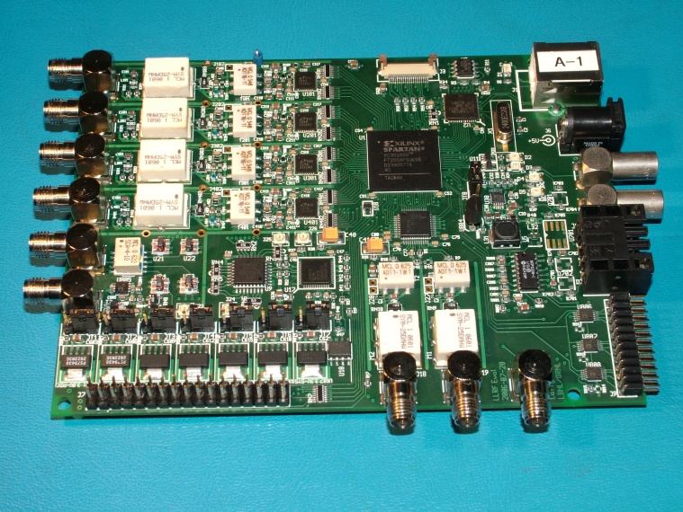
The poster titled "Hypothetical Design for ILC LLRF Hardware" was well received at the LLRF05 workshop in Geneva. While that cartoon of a circuit board is not an appropriate next step to actually build, progress towards that end requires testing of its parts and concepts. This note describes an LLRF evaluation board in the bring-up phase that could prove useful in that regard. This board is also discussed in the Linac-2006 paper/poster THP004.
The board now communicates over USB, loads FPGA bitstreams, acquires ADC data (2.05 bits rms noise with no signal applied) and makes IF waveforms from the DAC output. It has unexplained behavior in its LO distribution tree.
This board shares much of its conceptual design with the SNS Interim board, but there are many practical differences, mostly due to four years advancement in calendar time.
| Interim | Production | Evaluation | |
| IF ADC Channels | 4 x ADS809 | 4 x AD6645 | 4 x LTC22xx |
| IF DAC Channels | 1 (DAC902) | 1 (DAC904) | 2 (ISL5927) |
| FPGA | XC2S200 | XC2V1500 | XC3S1000 |
| Host interface | Ethernet | VXI | USB |
| Board Size | 5.2 x 5.4" | 3.8 x 11.9" | 3.8 x 5.0" |
| Board Layers | 8 | 12 | 6 |
| BGA packages | No | Yes | Yes |
| Power consumption | 8.0 Watts | 10 Watts? | 5.5 Watts |
| Input signal | IF | RF | RF or IF |
| Output signal | IF | RF | RF or IF |
Besides the component changes, several new or improved features have been incorporated:
The document linked to below walks through the board design:
Ideas that will not be tested in this evaluation board, but do need testing somewhere before the suggested ILC design can be considered safe:
The four-input-channel configuration is appropriate for studying several applications:
Firmware and software need to be developed for this board. Much of the SNS base still applies, and the core infrastructure for the USB interface has been tested on another project. These two halves will have to be carefully glued together. The board will boot and have its FPGA programmed via USB in three seconds.
Quantity 12 of the bare PCB have been manufactured (by Hughes Circuits), and six boards have been loaded (by IES, Inc). With all ADCs and DAC turned on, and clocking at 50 MS/s, the board draws 800 mA from +5V. Design errors discovered so far:
Wishlist items:
Larry Doolittle, LBNL
November 7, 2006