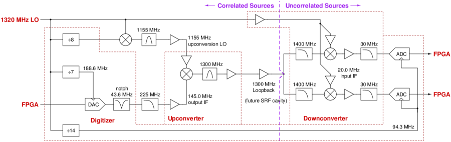
This is essentially a DAC driving two ADCs, with a lot of frequency conversion in between. By looking at the correlation between the two ADC signals, we extract the noise contribution before and after the signal split. The application of this hardware will be LLRF control of a 1300 MHz SRF cavity, which requires receive and transmit of 1300 MHz signals, with feedback routed through DSP implemented in the FPGA.
(click diagram for PDF) This diagram is an essentially complete description of the signal chain, just leaving off connectors, attenuators, coupling capacitors, bias tees, power supplies, and details of the filters.
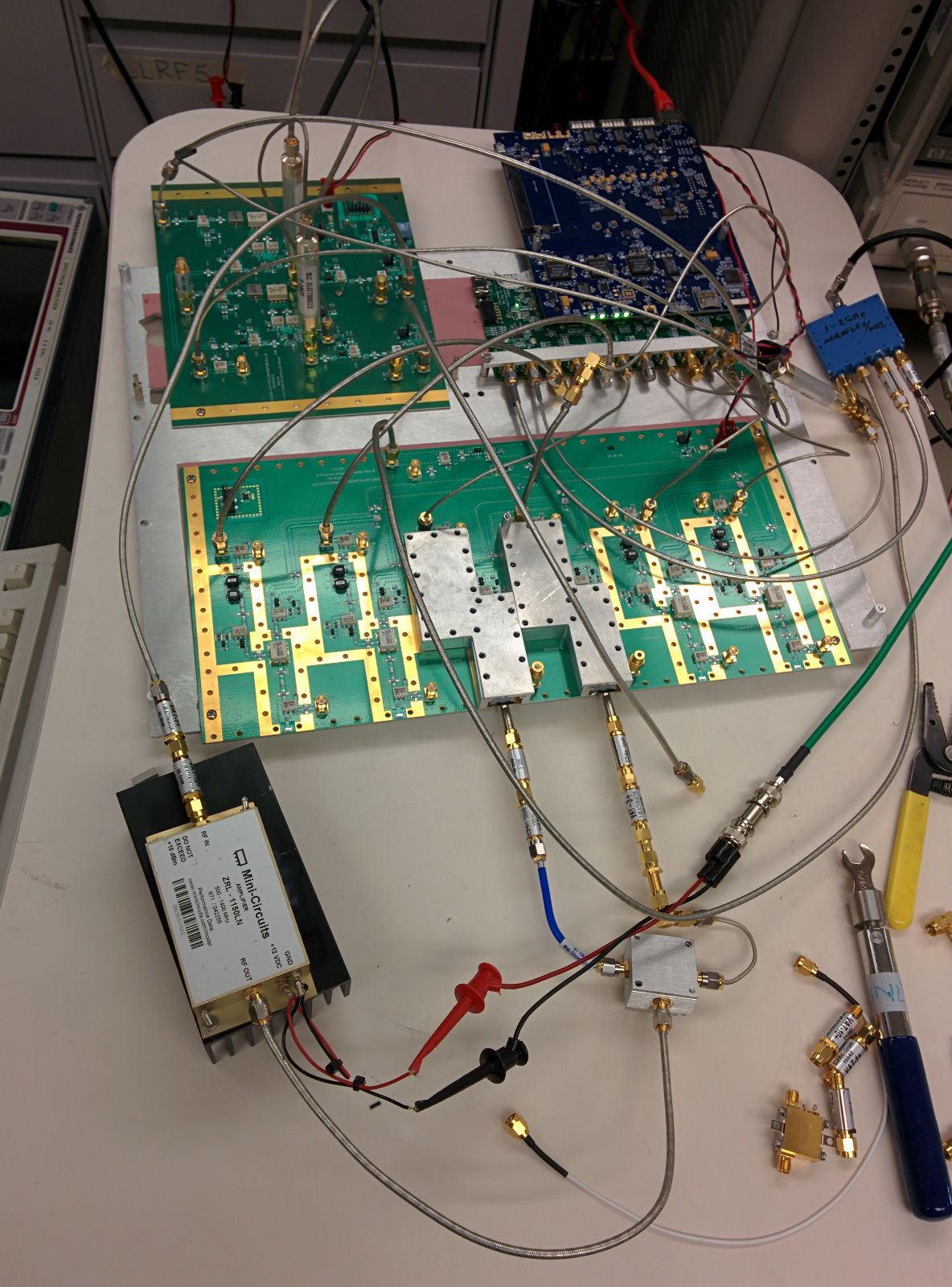
(click photo to enlarge)
A 203/264 (non-binary) NCO drives the DAC at a 188.6 MHz clock (derived from the 1320 MHz LO with an LMK01801 divide-by-7). This produces 145 MHz, which is mixed up to 1300 MHz and then back down to 20 MHz.
The ADC receives 20 MHz with a clock of 94.3 MHz (derived using a divide-by-14 output of the same LMK01801). Note that 20 MHz = 7/33 * the ADC clock. So while we acquire 8K points (only 8191 saved to the file, for boring reasons), the relevant FFT point count is 8184, so as to have a factor of 33 and not need a window function to turn both the 20 MHz carrier and all likely DAC and ADC spurs into single FFT bins.
Simultaneous sets of 8K raw AD9653 ADC results were acquired on two channels of the Digitizer board attached to a BMB-7, and transferred over Spartan-Ethernet to a host computer. 396 such data sets were acquired over a span of about 8 minutes, and saved to individual files. Each file has 8191 lines, with two decimal ASCII values each. Each ADC value is given as a 16 bit signed integer.
Download these raw data files in your choice of compression/archive format:
After the data files are unpacked from the above, a simple Octave .m file (make_plot.m) file produces the plot. MATLAB probably works, too.
Really very simple; label the waveforms of the two ADCs as x and y. Compute
S_xx = < FFT(x) ⋅ FFT(x)* >
S_yy = < FFT(y) ⋅ FFT(y)* >
S_yx = < FFT(y) ⋅ FFT(x)* > (DAC + upconverter)
diff = S_xx + S_yy - 2 ⋅ |S_yx| (downconverter + ADC)
where S_xx and S_yy are ordinary power spectra, and S_yx is known as the cross-correlation spectrum, explained persistently by Enrico Rubiola.
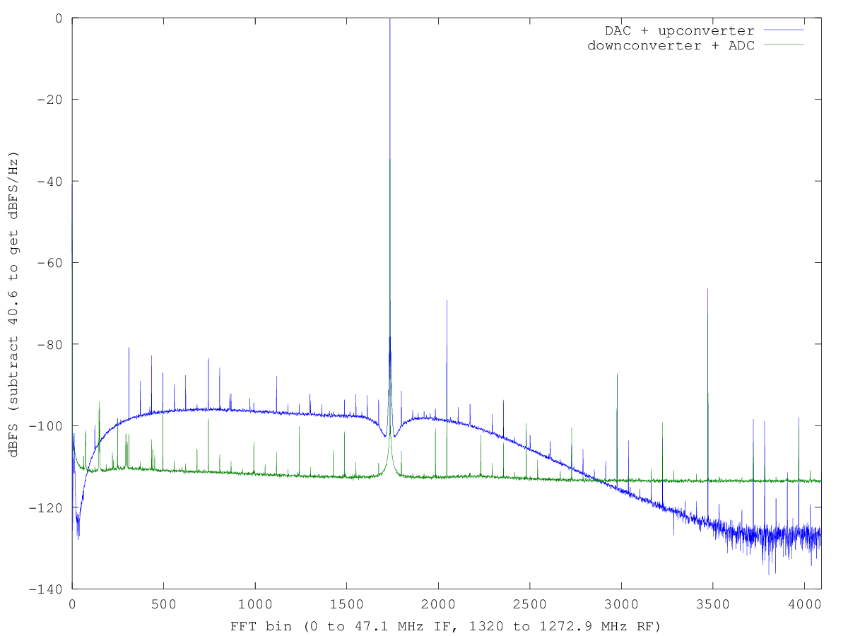
(click spectrum to enlarge)
A different view of the data can be generated by digitally mixing the waveforms down to baseband with a 7/33*f_clk formal local oscillator. This allows visualization of separate amplitude and phase noise spectra. Again, a .m file (ampm.m) is used to produce the plot below.
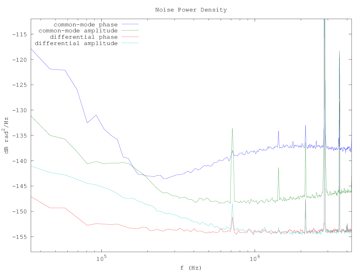
(click spectrum to enlarge)
The synthesized signal of interest is nearly 0 dBFS at FFT bin 1736. The expected spurs from the 14-bit DAC are present at the -84 dBc level, and from the 16-bit ADC at or below the -96 dBc level.
The strongest spur is the 2nd harmonic, at FFT bin 3472. The clock spur from the DAC is also visible in FFT bin 2046. This is an interesting case, since it is really a 1343.6 MHz line that downconverts to 23.6 MHz.
The -153 dBc/Hz noise floor measured for the two receiver channels (summed) makes approximate sense, and its flatness tells us that it's from the ADC, not the preamp (which would show the 30 MHz low-pass response). The shape of the DAC noise spectrum makes sense, following the 30 MHz low-pass filter. Its -138 dBc/Hz level is about 15 dB higher than expected (although still hugely better than demanded by this application). And I can't begin to explain the dip in noise near (0.8 MHz) the carrier in the DAC spectrum.
From the equal broadband amplitude and phase ADC noise levels, we deduce that noise floor is simple sample noise, and therefore ADC clock noise is not a significant contributor. The broadband output channel noise does not have that symmetry, so something in that hardware produces excess phase noise. That could be clock noise, since the output DAC is conceptually 7.25 times (145/20, 17.2 dB) more sensitive to clock noise than is the ADC.
The phase of the two IF signals was aligned in hardware to within about 1 degree. Without this step, all the spectra still come out looking reasonable by themselves, but the diff result is not believable.
Much of the experimental work and FPGA programming was done by Gang Huang.
Technical support by Kerri Campbell.
Upconverter and Downconverter boards supplied by Ed Cullerton of FNAL.
The BMB-7 was supplied and supported by John Jones.
The digitizer board was designed and tested as a team effort, including myself, Gang Huang, Jin Yang, and Yilun Xu at LBNL; plus Kathy Pham and Tung Phan at SLAC.
April 26, 2016, updated May 2, 2016
Larry Doolittle