World-Wide LLRF links
Other LLRF (Low Level RF) groups around the world:
SNS LBNL LLRF
A quick collection of pointers to documents relevant to LBNL's implementation
of an LLRF system to run the SNS rebuncher cavities.
Generation 1
- Linac 2002 conference paper: "The SNS Front End LLRF System"
- A numerical model of the system,
including cavity and high power RF.
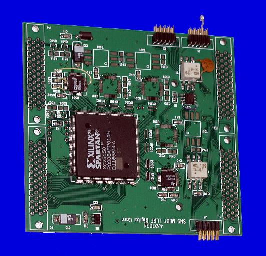
- Documentation of the register map implemented
in the Xilinx XC2S150.
- Summary of the needed network services to
bring up the embedded computer.
- How to build Linux from
scratch to run on the embedded nanoEngine
- Schematic of the LLRF digital board (PostScript, actually
the native file for XCircuit).
- Engineering changes to the LLRF digital board.
- Interfaces (pinouts and signal levels) between
the digital board and the rest of the system.
- Cable mods for the connection between the analog
and digital boards.
- Channel mapping for the 16 ADCs and 16 DACs
provided on the analog board.
- 3/30/2002 snapshot of the
support software and VHDL firmware. This has been replaced by an EPICS layer
based on xcas, which is checked into the SNS project CVS.
- 7/12/2002 snapshot of the VHDL firmware,
now adapted to Foundation 4.2, but not tested on hardware.
- jtag-utils is the
software used to download firmware to the FPGA.
- Key data sheets:
- AD9765, 125 MS/s 12-bit dual DAC.
- ADS808, 70 MS/s 12-bit ADC.
- XC2S150, 3456-cell FPGA with 6 kBytes RAM.
Generation 2
Five copies of a revised system have been constructed,
based on a more integrated board.
I will post more information as it becomes available.
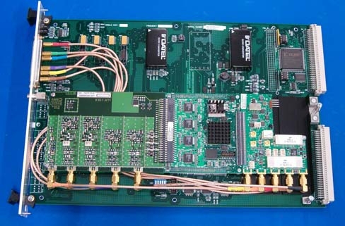
- Photographs of the assembled chassis.
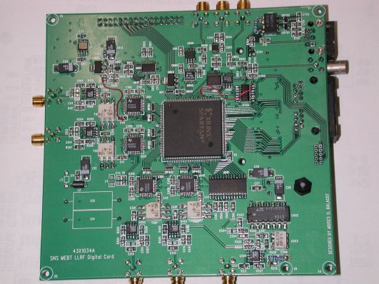
- Schematic of the LLRF digital board (PostScript, actually
the native file for XCircuit).
- Plan for a 50 MHz Analog Output Channel
- PAC 2003 paper: Operational Performance of the SNS LLRF Interim System
- Key data sheets:
- DAC902, 165 MS/s 12-bit DAC.
- ADS808, 70 MS/s 12-bit ADC.
- XC2S150, 3456-cell FPGA with 6 kBytes RAM.
- Verilog
(somewhat outdated; see SNS CVS for the latest)
- Measurements of the system's phase stability.
- Verilog support for three generations of hardware,
complete with exhaustive test benches and host support:
llc-suite
Generation 3
Field Control Module (FCM) board stack:
- Digital Front End (DFE) created by Matt Stettler (LANL)
- Analog Front End (AFE) created by Bergoz
- RF Output (RFO) created by John Power (LANL)
- Motherboard created by Mark Prokop (LANL)
Programming:
- FPGA code and Hardware Abstraction Layer (HAL) by Larry Doolittle (LBNL) (llc-suite)
- EPICS driver, screens, and sequencers by Kay-Uwe Kasemir (ORNL)
Advance thoughts
Created March 8, 2002
Last update April 28, 2009
Larry Doolittle